
JTAG and SWD: debug interfaces from the attacker’s side

During development, the debug port is the firmware team’s most valuable tool. It lets you halt the processor, read memory, set a breakpoint and reprogram the board in seconds.
In production, that same port offers exactly the same possibilities to whoever holds the device. The only difference is that they were not invited.
JTAG and SWD in two minutes
JTAG (IEEE 1149.1 standard) was originally designed to test the solder joints of electronic boards. It has become the standard debug interface of most processors. It uses four signals, TCK, TMS, TDI and TDO, sometimes complemented by a reset line.
SWD (Serial Wire Debug) is the alternative offered by Arm for Cortex microcontrollers. It provides the same debug functions with only two signals, SWDIO and SWCLK. It is the interface found on virtually all STM32, nRF and other Cortex-M microcontrollers.
Both give access to the heart of the system: processor registers, RAM, flash memory, peripherals.
What an open debug port allows
- Extracting the complete firmware. This is the most common use, and the starting point of any reverse engineering. The secrets it contains follow. See Secrets in the firmware: three flaws, one root cause.
- Reading RAM during execution. Session keys, decrypted passwords and data being processed are found there in clear.
- Bypassing a check. Halting the processor just before an authentication test, modifying a register, resuming execution.
- Reprogramming the device. Replacing the firmware with a modified version, then putting the device back into circulation.
- Cloning the product. A firmware extracted and copied onto an identical board gives a working device.
The analysis we published on the attack on Danfoss controllers is a reminder: a password algorithm hidden in a firmware is not a secret, because the firmware always ends up being extracted.

How an attacker finds the port
The debug connector is almost never labeled on a finished product. That does not slow an auditor down much.
- Visual inspection. A 10- or 20-pin connector, a row of unpopulated pads, a few test points lined up near the microcontroller.
- Datasheet. The microcontroller part number gives the pins assigned to debugging. All that remains is to follow the traces.
- Measurements. A multimeter identifies ground and power, which reduces the number of candidates.
- Automated search. Dedicated tools try every pin combination until the component returns a valid response.
- Connection. An off-the-shelf debug probe and open-source software are enough to talk to the target.
Removing the connector or hiding the pads is not protection. The signals are still present on the component’s pins.
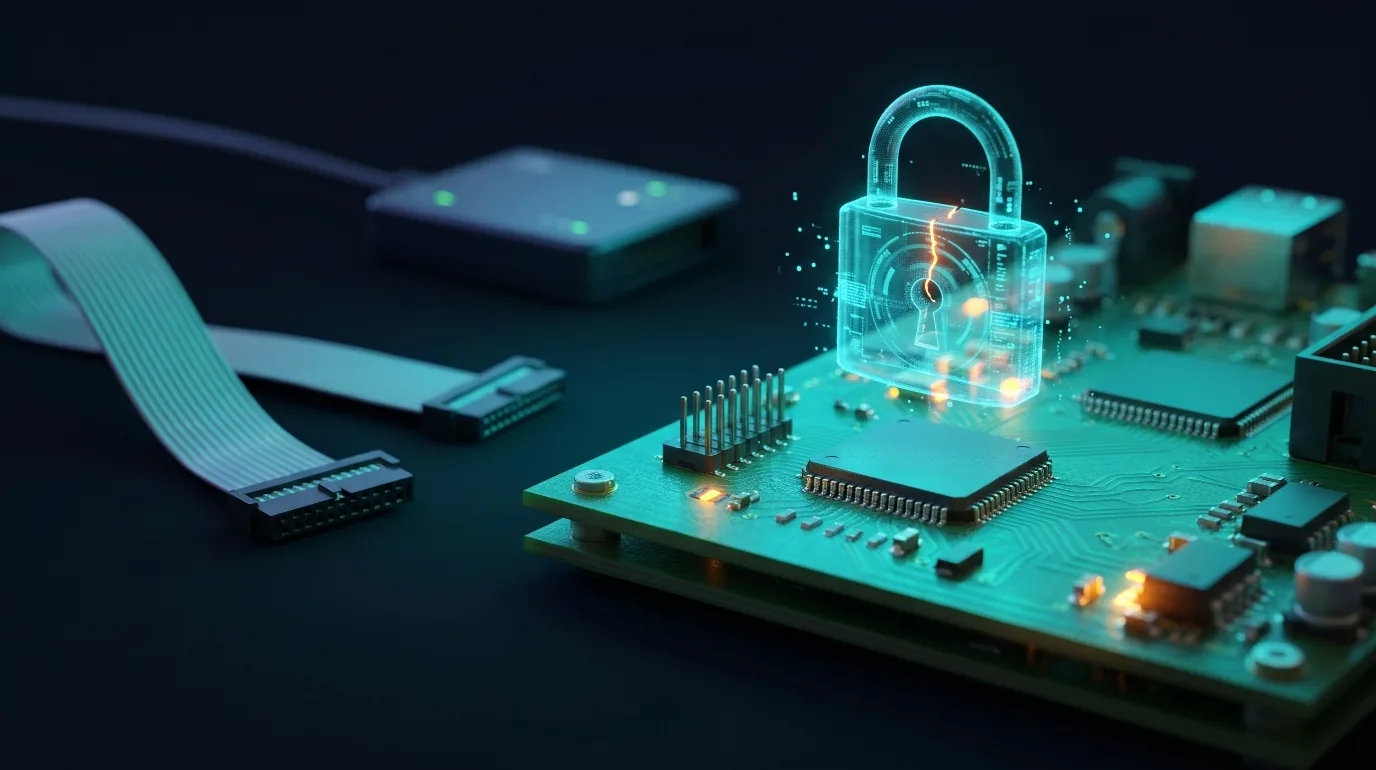
Locking it, and what that is really worth
Microcontroller manufacturers provide protection mechanisms. They are not active by default: it is up to the product manufacturer to enable them at the end of production.
| Family | Mechanism | What it does |
|---|---|---|
| STM32 | Read protection (RDP) | Depending on the level, blocks flash reads through the debug port, or permanently disables that port |
| ESP32 | eFuses | Disables JTAG, combined with secure boot and flash encryption |
| nRF52 | APPROTECT | Blocks debug port access to memory |
Three honest clarifications are in order.
The levels are not equal. On STM32 parts that have it, the intermediate level leaves the port active and allows a rollback at the cost of erasing memory. Only the highest level permanently disables debugging. It is irreversible, which explains why many teams hesitate to enable it. Not all families offer this level.
These protections have been bypassed. Several public research papers have shown bypasses on various microcontroller families, through power glitching or by exploiting the boot sequence. These attacks require equipment and know-how, but they exist and are documented.
Locking the port does not replace the rest. If the firmware can be read another way (unencrypted external memory, unprotected update, chatty bootloader), locking debug protects nothing.
The design rules
- Enable debug port protection on every unit produced, and verify it at end of line with an automated test.
- Choose the protection level according to the threat model, and document that choice.
- Assume the firmware will be read one day. Put no secret shared by all devices in it.
- Use a unique key per device, so that compromising one unit does not compromise the fleet.
- Plan for returns to the workshop without reopening debug: a dedicated authentication mechanism, or board replacement.
- Combine debug locking, secure boot and firmware signing and storage encryption.
These points correspond to the attack surface reduction and protection against unauthorized access requirements of the Cyber Resilience Act, as well as to the IEC 62443-4-2 requirements on diagnostic and test interfaces.
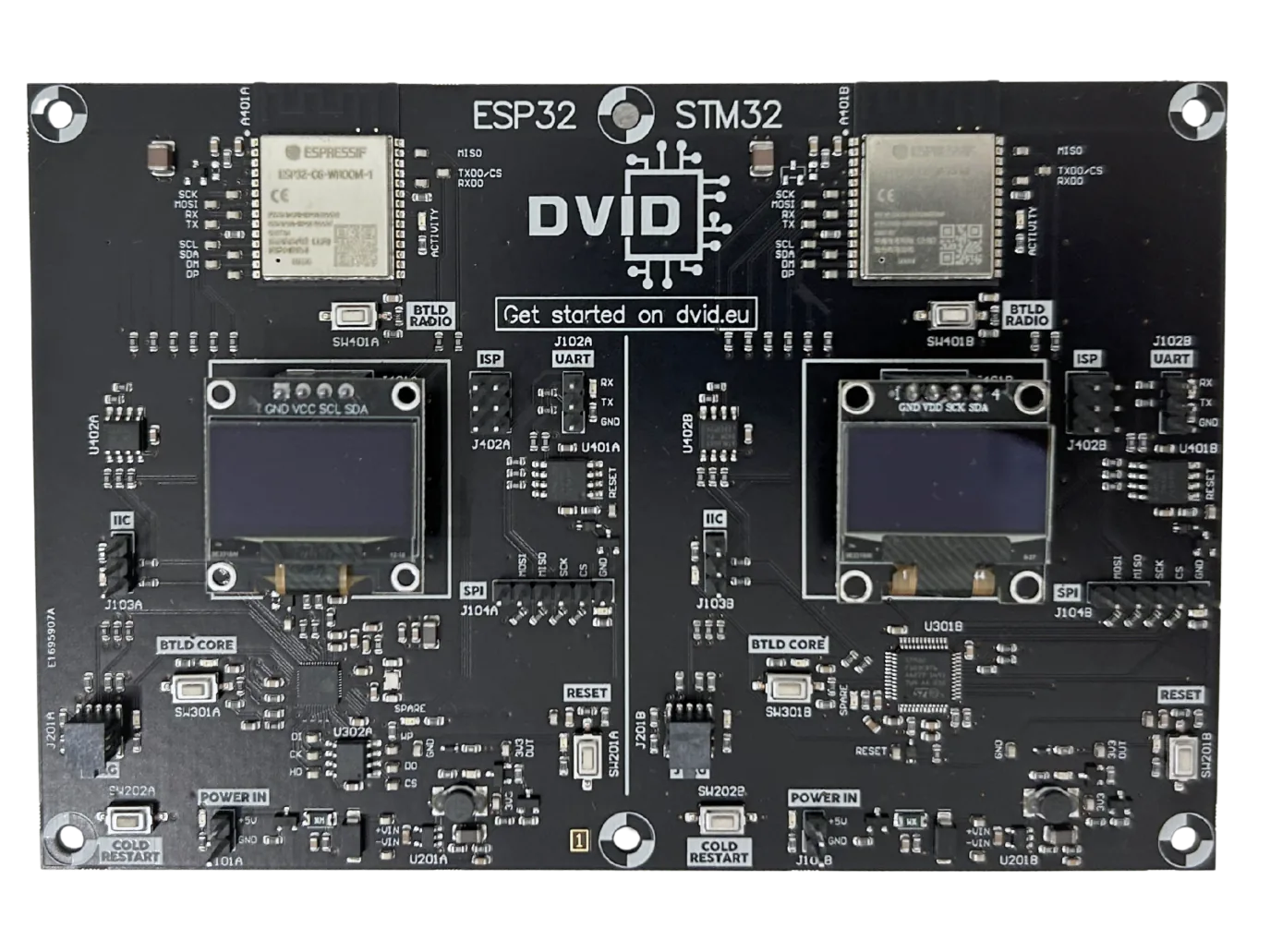
Practice it on the DVID board
The DVID board combines an ESP32 and an STM32, with a programming layer that exposes JTAG, SWD and UART. Two trainings are dedicated to these interfaces: an introduction to JTAG and a discovery of SWD on STM32.
Participants learn to:
- identify the debug pins from the datasheet
- connect a probe and establish communication with the target
- read memory and extract a firmware
- observe the effect of the protections when they are enabled
- formulate a locking recommendation suited to the product
Who is it for?
- firmware developers and industrialization managers
- pentesters and hardware auditors
- product security managers
- quality teams in charge of end-of-line testing
Further reading
See also I2C security: what an attacker reads on two wires and Exposed UART, vulnerable MQTT. To validate these skills, discover the DVID certification path.
Learn more: https://dvid.eu
Contact us: https://dvid.eu/#contact
Follow our news: https://www.linkedin.com/company/dvid/